SAHA INSTITUTE OF NUCLEAR PHYSICS
Department of Atomic Energy, Govt. of India
SINP Home Webmail Member Search A+ A A-
Log in
Surface Physics and Material Science
  Transmission Electron Microscope
      
   Transmission Electron Microscope
Description

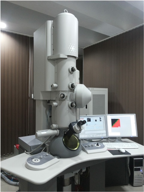
The transmission electron microscope is used to characterize the microstructure of materials with very high spatial resolution. Information about the morphology, crystal structure and defects, crystal phases and composition can be obtained by a combination of electron imaging (2.0 Å point resolution), electron diffraction, energy dispersive X-ray spectroscopy, Electron Energy Loss Spectroscopy with small (~ 1 nm) probe capabilities. The small probe can be positioned on very fine features in the sample for microdiffraction information or analysis of x-rays for compositional information. The spatial resolution for this compositional analysis in TEM is much higher, on the order of the probe size. Conversely the signal is much smaller as sample is very thin and therefore less quantitative. The high brightness field-emission gun improves the sensitivity and resolution of x-ray compositional analysis over that available with more traditional thermionic sources. The transmission electron microscope uses a high energy electron beam transmitted through a very thin sample to image and analyze the microstructure of materials with atomic scale resolution. The electrons are focused with electromagnetic lenses and the image is observed on a fluorescent screen, or recorded on digital camera. The electrons are accelerated at several hundred kV, giving wavelengths much smaller than that of light. However, whereas the resolution of the optical microscope is limited by the wavelength of light, that of the electron microscope is limited by aberrations inherent in electromagnetic lenses. A TEM specimen must be approximately 1000 Å or less in thickness in the area of interest. The entire specimen must fit into a 3mm diameter cup and be less than about 100 microns in thickness.

Manufacturer      

FEI Co. (Netherlands)

 Model

Tecnai G2 F30 S-TWIN

 Installation

October, 2012 at the ground floor of Phase III building

System Control

Instrument runs using the TIA interface, and additional software includes: Gatan Digital Micrograph (TIA-embedded version), Xplore3D (tomography package with data acquisition, Inspect3D, TrueImage (focal series reconstruction).

Resolution 2.0 Å point-to-point resolution, 1.02 Å line resolution, 1.4 Å information limit in TEM mode
0.75eV in EELS mode

Magnification

Magnification range in TEM mode: 60x - 1000Kx
Magnification range in STEM mode: 150x - 230Mx

Accelerating voltage

Flexible high tension (50, 100, 150, 200,
250, 300 kV and values in between)

Electron gun

Schottky Field emitter with high maximum beam current (> 100 nA),
High probe current (0.6 nA in a 1 nm
spot, 15 nA in a 10 nm spot)


Detectors

 HAADF detector from Fischione (model 3000)  and on-axis BF/DF detector

EDAX SUTW (super ultra thin window) and analyzer, 0.13 srad EDS solid angle

Energy Loss Spectroscopy (EELS) were carried out using a post-column Gatan Quantum SE (model 963)
Vacuum System

 Fully interlocked differentially pumped column

Clean vacuum system with turbo molecular pump, pre-pumping column, gun and specimen airlock

150 l/s Ion Getter Pump on specimen area

Vacuum levels: specimen chamber 2.7 x 10⁻⁵ Pa; gun 5 x 10⁻⁷ Pa

Stage movements

Fully computer-controlled, eucentric side-entry, high stability CompuStage

Choice of a variety of specimen holders

X, Y movement 2 mm, specimen size 3 mm

Specimen recall reproducibility ≤ 0.1 μm (x, y) and ≤ 0.1° (α tilt) attainable

Drift < 0.5 nm/minute with a standard holder

±40° tilt with double-tilt holder, ±70° tilt with tomography holder

Image media

Digital images are captured using Gatan Orius SC1000B CCD camera


Last Updated on Wednesday, 17 August 2016 14:28
Copyright © 2025 Saha Institute of Nuclear Physics. All Rights Reserved. Designed & Developed by UCDS