Activities
Multiplexed ANAlog Signal Processor (MANAS)
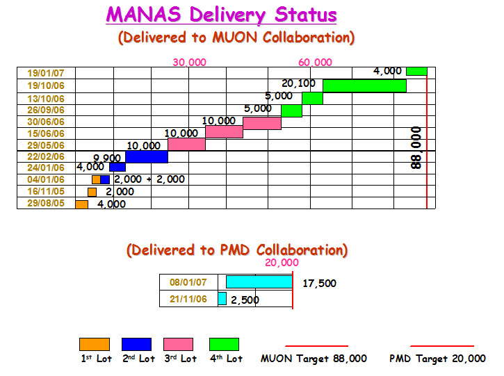
MANAS is the first large scale production of a mixed signal ASIC in India. The total quantity produced for the International Collaboration ALICE is 1,10,000 (88,000 for Dimuon Spectrometer and 22,000 for Photon Multiplicity Detector). The delivery has been successfully completed in January, 2007.This has been an extremely creditable performance on the part of SCL and this is the first time that a fully indigenous high-technology device is being delivered to CERN.
|
Organization |
Job Description |
|
SINP, Kolkata |
Front-end Design, Circuit simulation, MANAS bias-conditions, Automatic Test Board validation, MANAS testing and validation of production batches |
|
AMU,Aligarh |
MANAS testing and validation |
|
SCL, Chandigarh |
Back-end Design,Setting-up of the Automatic Test Bench,Wafer Fabrication |
|
UTAC, Singapore |
Wafer testing, packaging and device testing |
Concept
The front-end of the readout electronics consists of 16 � channel each consisting of a preamplifier (a charge amplifier), shaper circuits, analog switches including track and hold stage and digital multiplexer circuit. Preamplifiers are especially designed to be close to the detector to preserve the maximum signal-to-noise ratio, and to accept the signal from a detector with minimum distortion. The optimum configuration of the `front-end� of the preamplifier is dependent on the characteristics of the detector being used. Total circuit is targeted to be accommodated in an analog-digital mixed signal VLSI chip. MANAS is the first large scale production of a mixed signal ASIC in India. The total quantity produced for the ALICE Collaboration is 1,10,000 (88,000 for Dimuon Spectrometer and 22,000 for Photon Multiplicity Detector).
Foundry Identification
Before performing the circuit level simulation we had to identify the foundry in which the chip has to be fabricated. Only after getting the process parameters we could proceed for its simulation. The VLSI foundry at Semiconductor Complex Limited, a Government of India Undertaking, was identified for our job. It was further decided that the fabrication would use SCL 1.2?m CMOS N-well technology.
Software
Before performing the circuit level simulation we had to identify the foundry in which the chip has to be fabricated. Only after getting the process parameters we could proceed for its simulation. The VLSI foundry at Semiconductor Complex Limited, a Government of India Undertaking, was identified for our job. It was further decided that the fabrication would use SCL 1.2?m CMOS N-well technology.Work Schedule
Before performing the circuit level simulation we had to identify the foundry in which the chip has to be fabricated. Only after getting the process parameters we could proceed for its simulation. The VLSI foundry at Semiconductor Complex Limited, a Government of India Undertaking, was identified for our job. It was further decided that the fabrication would use SCL 1.2?m CMOS N-well technology.
- i) Circuit level simulation of the whole schematic of chip including the digital part was completed in May 1999.
- ii) Layout, parameter extraction and layout simulation were completed in September 1999.
- iii) PG tape for MANAS16 was released on October 1999.
- iv) First batch of prototype were released in March 1999,
- v) Wafer level testing was in progress in March 1999.
- vi) First batch of tested MANAS 16 packaged in 48-pin ceramic package was expected in July 1999.
- vii) Prepproduction batch of 2000 MANAS chips- August 2002
- viii) Production Readiness Report- Nov 2002
- ix) Initiation of wafers Production at SCL-April 2004
- x) Validation of Automatic testing facility at Singapore by the Saha Instituteteam March 2005
- xi) Validation of the production batch August 2005
- xii) Final acceptance of ALICE collaboration for NANAS as the sole readout chip for Muon spectrometer October2005
- xiii) First Delivery batch Jan 2007
- xiv) Completion of Delivery of 1,08,000 tested chips Jan 2007
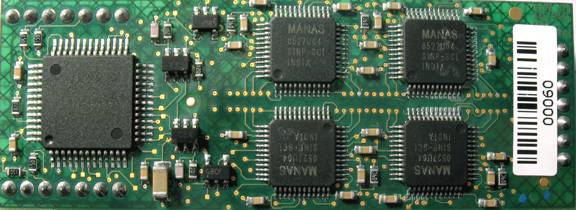
The chip has a die size of 2.6 mm X 4.6 mm containing 5000(app) MOS transistors consuming a total of less than 150 mW of power
Packaged dimension 7 mm X 7 mm
Analog-Digital Chip - ~ 10, 000 Transistors
16 channel readout
")
")