Commissioning tests of the 2nd Muon Tracking Station of ALICE
The Muon Spectrometer of ALICE will track the decay muons from the heavy quarkonium states (J/Y, U, U’, U”) through five tracking stations. The suppression of the production of these quarkonium states in ultrarelativstic heavy ion collisions is believed to be one cleanest signal of the Quark Gluon Plasma state. The spectrometer has an angular coverage from 171° to 178° and thus will detect low pT events which originate from the primordial soup.
The Second Tracking Station is placed at 6.86 meter from the Interaction Point and thus has an outer radius of 117 cm.
The station comprises of eight Cathode Pad Chambers with a total of 2,26,817 readout channels. The analog pulses for each channel are shaped by MANAS chip, which is an indigenous chip fabricated at Semiconductor Complex laboratory at Chandigarh. All the detectors have been successfully installed at the experimental cite in a 54 meter deep pit [1].
The commissioning tests were carried out during January-February, 2008 were:
1. Gas Leakage Tests2. High Voltage (HV) Tests
3. Electronic Read Out Tests
4. Electronics Gain Measurement for every channel
Gas Leakage Tests
All the chambers of the Muon Spectrometer were fed with a 80% Ar + 20% CO2 gas-mixer from a gas-rack. Every input and output channel of this rack was fitted with a flow meter. The difference of these readings was a measure of observed gas leakage in every channel. It had been found that all the chambers of the 2nd station had a leak rate of less than 8% with a flow rate of 5 liter/hour. This leak rate is acceptable considering the long length of gas piping and large number of gas couplings.
HV Tests
The High Voltage tests were carried out after a week of gas flow through the chambers. All the chambers showed negligible leakage current (less than 3 nA) at 1650 Volt except one chamber which had a leakage current ~ 35 nA. Thus, it was decided to operate all the chambers of second station at 1625 Volt. It is to be noted that the proportional plateau for MIP particles in these chambers extends from 1575 V to 1700 V.
Electronics Read Out Tests
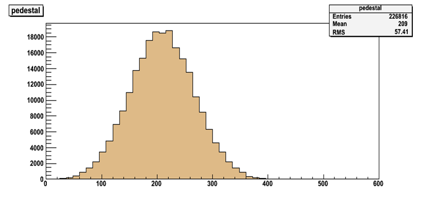
The readout test for every channel was carried out by measuring the output pulse with no input. These measurements are called Pedestal runs and were carried out 500 times to find the mean value for every channel. This test validates the address assignment to every readout card (MANU) and the proper transmission of signal to DAQ. Fig. 1 (a) shows the histogram of the pedestal level of all the readout channels. This distribution is quite nar row which is essential for a large dynamic range for every channel. It is to be noted that 1 ADC channel = 0.6 mV.
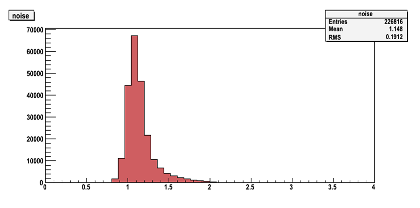
These detectors do not have any metallic frame in order to minimize the radiation length. Thus, it was a challenge to develop a good grounding scheme for these large area detectors so that the electronic noise could be minimized. The electronic noise is defined as the sigma value of the Gaussian distribution fitted to the 500 pedestal values for every channel. The measured noise histogram for all the readout pads after the chamber installation is shown in Fig. 1 (b). The mean noise is found to be only 0.7 mV which establishes that grounding scheme has been satisfactory.
Electronics Gain Measurement
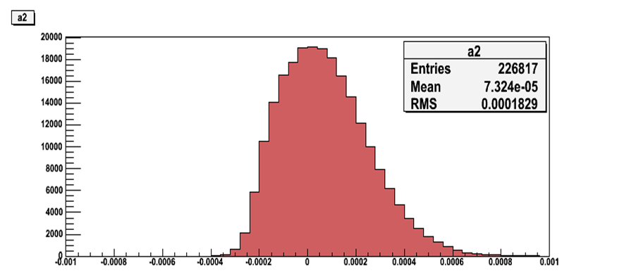
To measure the electronic gain for every channel, the output voltage levels were monitored for 10 different input charges. The charge injection was done through the calibration line of MANAS chip. The input charges were varied from 0 fC to 450 fC at a uniform step size of 50 fC. For every charge injection, the average value of 500 measurements was stored for each of the 2,26,817 channels. For every channel, the mean voltage level measured at 0 fC was subtracted from the values measured with specific input charges. The calibration points for every channel were fitted with a second order polynomial of the form a1 x + a2 x2 where x is the ADC channel. Fig. 2(a) shows the histogram for the linear coefficient.
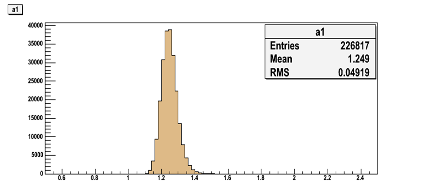
The observed gain spread was 4% (RMS/Mean). The spread will be corrected through gain calibration for every channel. It is interesting to note that the observed non-linear coefficient (Fig. 2(b)) is quite small and thus establishing a linear response of MANAS chip over a wide input range of charge up to 450 fC.
The commissioning of Station 2 has been successfully completed. The electronics readout tests also proves the satisfactory performance of MANAS chip after its integration to the full readout sequence.
References[1] DAE-BRNS Symposium on Nuclear Physics, 52 587 (2007)